Welcome to the Integrated Atom Chip (IAC) group.
We aim to develop the miniature components and underpinning technologies that will transform ultra-sensitive quantum-enabled measurement and information processing mechanisms ('atom chips') from laboratory demonstrations into practical integrated devices.
Quantum technology based on the stranger aspects of quantum physics ("Quantum 2.0") are expected to become the next-generation tools for timing, sensing, navigation, processing and communication in the coming decades. Many processes use ultracold atoms as they are arguably some of the purest quantum states available to us due to their decoupling from the incoherent 'classical' environment.
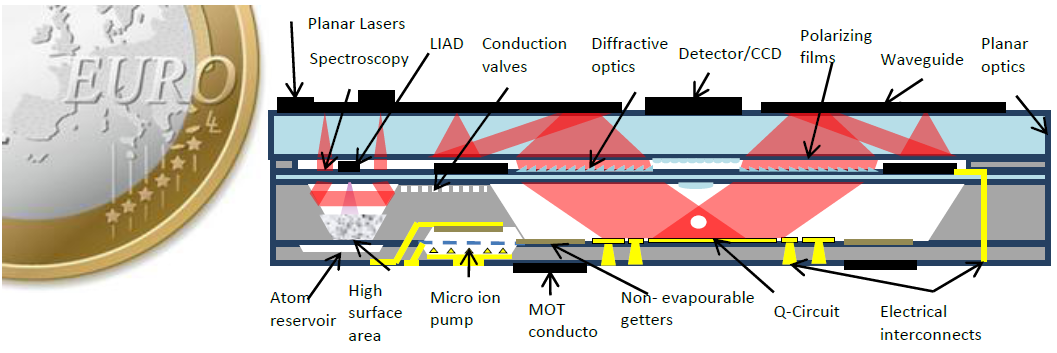
Cold atom experiments come in many forms, usually in large scale vacuum chambers too bulky for practical devices beyond the laboratory, but many are being translated to more compact forms known as 'atom chips'. These are microfabricated wires patterned onto a substrate through which currents are passed to form various magnetic traps for atoms. See XXX for a review. Currently these chips, which are no larger than a postage stamp, are still housed in large vacuum chambers surrounded by a vast array of optics, laser, detectors and control electronics. If Quantum Technology is to truly make a significant impact we need to focus on miniaturizing and integrating this infrastructure as well. We aim to do this not with scaled-down copies of conventional components, but with mass-producable planar fabrication techniques, developed for semiconductor devices and MEMS, which we adapt to perform the roles of large scale apparatus.

The image above depicts an idealised vision of how an atom chip can be fully integrated into a stand alone devise. There are numerous technologies which must be miniaturised but also made compatable with one another during the manufacturing process. These include: vacuum chambers, pumps and gauges, controllable atom sources, stabilized lasers, optical and electrical interfaces, micro optics and beam guiding, and detection.
For more information on how we plan to do this, please explore the Research pages.
This project is at the boundary of Physics and Engineering and hence it is a multidisciplinary collaboration within the University of Southampton involving the School of Physics and Astronomy, the School of Electronic and Computer Science (ECS), and the Optoelectronics Research Centre (ORC). We also have additional links to the School of Chemistry and the Engineering Sciences unit.
Website updated: 10/07/2014


